Rgmii Layout
The p2041 rgmii implies that pc board design requires clocks to be routed such that an additional trace delay of greater than 1.5 ns is added to the associated clock signal. Take a look at this article to see more guidelines on the various mii standards.
RGMII interfaces (KSZ9031) Code World
The device also integrates mdi interface termination resistors into the phy.
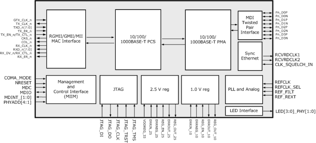
Rgmii layout. The rgmii specification requires that the signal clock be delayed by 1/2 bit time (2 ns) at the receiving end of the data path. I have a similar question to dp83867ir: The ksz9031rnx provides the reduced gigabit media independent interface (rgmii) for direct connection to rgmii macs in gigabit ethernet processors and switches for data transfer at 10/100/1000 mbps.
Rf layout comment it is strongly recommended to follow our reference layout exactly for the pa output matching and pa supply layout since that will impact output power, evm and emi. The document has moved here. By default, rgmii and rtbi modes operate using 3.3v i/o power supply.
Rgmii gtx_clk 33 i, pd rgmii transmit clock, 125 mhz digital. Rgmii_rxd3 10 rgmii_rxd2 11 rgmii_rxd1 12 rgmii_rxd0 13 rgmii_rxck 14 rgmii_rxctl 15 rgmii_reset 16 rgmii_clkin_125m 17 bt_uart_cts 1 rgmii_txck 18 rgmii_txd3 19 rgmii_txd2 20 rgmii_txd1 21 rgmii_txd0 22 rgmii_mdc 23 ephy_clk_25m 24 rgmii)txctl 25 rtgmii_mdio 26 csi0_sda 27 csi0_sck 28 ts/ncsi0_d13 29 ncsi0_d12 30 vbat2 31 rtc 32 acin1 33 acin2. Adding a 22 damping resistor is recommended for emi design near mac side.
The best technique varies according to the design. I.mx layout recommendations application note, rev 1.0 4 freescale semiconductor figure 3 fiducials 2 placement there are many techniques for placement such as by circuit type, by schematic page, by most critical components, and so on. In fact, i don't know.
This high port count switch uses a main controller icm that includes the mac and integrated phy layer. The cadence ip supports both Always follow the layout guidelines in the datasheet for the phy device you are using in your pcb when planning your layout.
However, these other standards, particularly gmii/rgmii, use 125 mhz clock. First, analyze and understand the schematic. For the rgmii signal below 0.5 ns, this should be a.
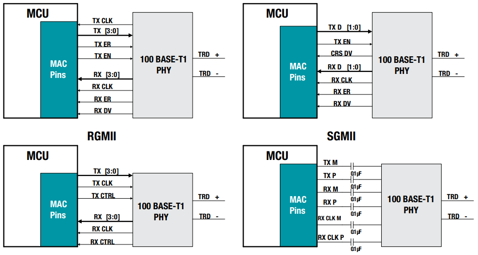
Rgmii version 1.3 uses 2.5v cmos, whereas rgmii version 2 uses 1.5v hstl. The ksz9031rnx provides the reduced gigabit media independent interface (rgmii). The image below shows an example portion of a layout for an ethernet switch.
The principle objective is to reduce the number of pins required to interconnect the mac and the phy from a maximum of 28 pins (tbi) to 12 pins in a cost effective and technology independent manner. The rgmii interface is the physical connection between the ethernet phy and the ethernet mac. Rx_clk 31 i/o, pd 125mhz digital, adding a 22 damping resistor is recommended for emi design near phy side.
Readers must be very curious about what this board is for. Mii or tbi digital interfaces. Ball a1,b2(d1,e1) is tx0(tx1) pa differential output, so its trace should be.
If you are using the ethernet fmc, the phy is the marvell 88e1510, and the ethernet mac is inside the fpga.the rgmii interface is a dual data rate (ddr) interface that consists of a transmit path, from fpga to phy, and a receive path, from phy to fpga. The rgmii is intended to be an alternative to the ieee802.3u mii, the ieee802.3z gmii and the tbi. The figure below is a multi port phy developed and designed by the author for a friend, which is connected to the external mac board through a row of pins.
Mii and rmii routing guidelines. In order to accomplish this objective, the data. An optional 2.5v power supply can be used as well for rgmii and rtbi modes, as specified by the rgmii/rtbi standard.
Although mii and rmii use relatively low data rates, the limiting parameter that determines whether a trace. It uses differential pairs at 625 mhz clock frequency ddr for tx and rx data and tx. Refer to mii register 23 in the vsc8204 datasheet for.
Rx_dv 30 i/o, pd rgmii receive data valid rxd0 29 i/o, pd rgmii received data 0 Many phy vendors already incorporate the necessary delay inside their chip.

RGMII wiring guide RGMII Layout Guide Programmer Sought

Briefly on FPGAbased Gigabit design Programmer
Solved MMCM config issue in Vivado 2017.1 f

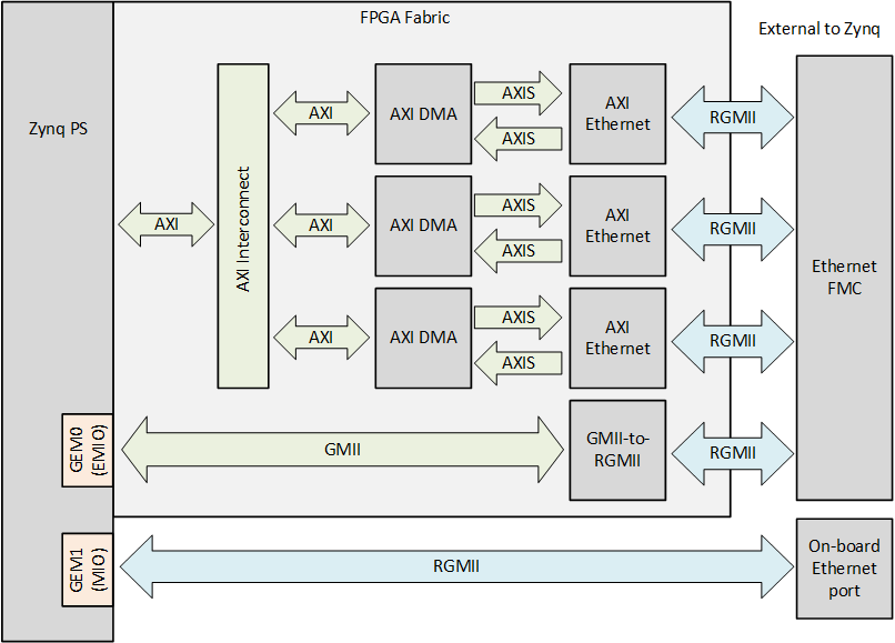
Description — Zynq GEM Reference Designs documentation

Can PL receive data from the output of GMII to RGM
Solved correct usage of Gmii to Rgmii IP Community Forums


Rgmii Layout Guidelines PCB Circuits
RGMII布线指导 RGMII Layout Guide 无线时代

Rgmii Layout Guidelines PCB Circuits
Axi Subsystem + Gmii to Rgmii RX path i

![]()
KSZ8795CLXDEVAL Reference Design Interfaces
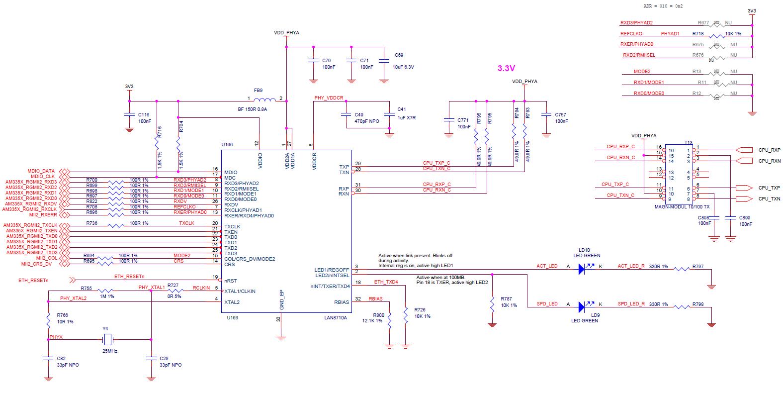
[Resolved] AM335X RGMII and RMII PHY configuration
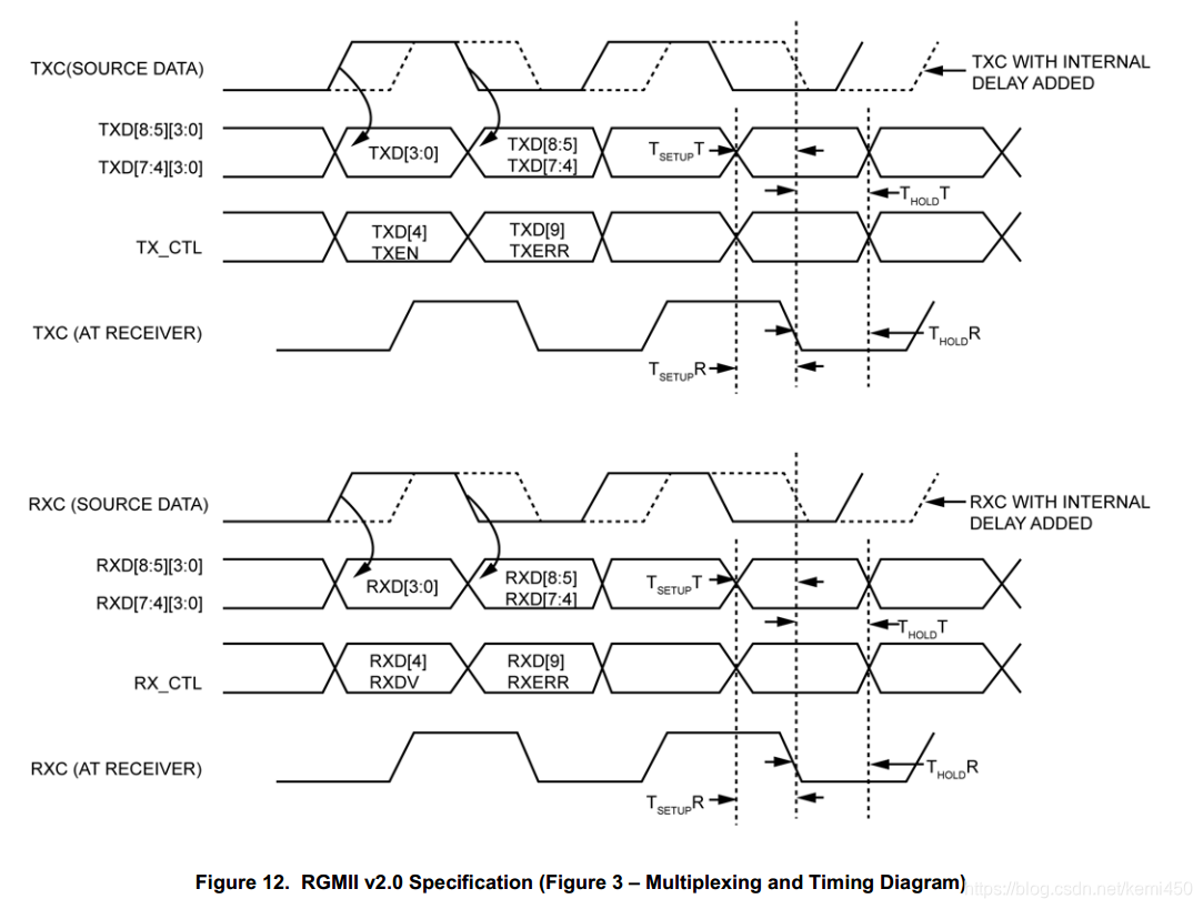
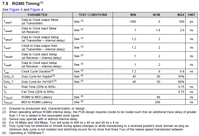
RGMII Interface Timing Considerations FMC

Example designs FMC


RGMII布线指导,RGMII Layout Guide 无线时代

CN0506 HDL Reference Design [Analog Devices Wiki]
DP83867IR RGMII timing questions Interface forum
Automotive Present and Future Design

DP83867IR RGMII timing questions Interface forum